Defining High Power in Laser Optics

High-power lasers are at the core of modern technological advancement, powering a wide range of applications from industrial material processing techniques like welding, cutting, drilling, soldering, marking, hardening, and surface modification, to precision tools in medicine, military-grade directed energy systems, and cutting-edge research such as particle acceleration and laser-induced nuclear fusion. Understanding and defining high power in laser optics is crucial for these diverse applications.
There is currently no universally accepted definition of what is considered “high power” in laser systems, as performance limits depend strongly on the application, pulse regime, and damage mechanisms involved. Defining High Power in Laser Optics therefore requires shifting the focus from output power alone to Laser-Induced Damage Threshold (LIDT), absorption control, and coating technology tailored to real operating conditions. The classification therefore is relative and shaped by the specific application. In industrial manufacturing, high power often implies multi-kilowatt outputs. In laser material processing, it typically refers to several kilowatts or at least a few hundred watts. Meanwhile, display technologies may define high power as just tens of watts, and in consumer electronics, like laser pointers, a few hundred milliwatts can qualify. For pulsed lasers, the picture becomes even more nuanced, as peak power, determined by pulse duration and repetition rate, can reach extreme levels even when average output remains moderate.
We asked our LinkedIn audience what they consider high power, and the majority defined >100 W as the threshold for high power. However, for some, only the sun is able to reach high power. You can see the results of our poll in Figure 1.
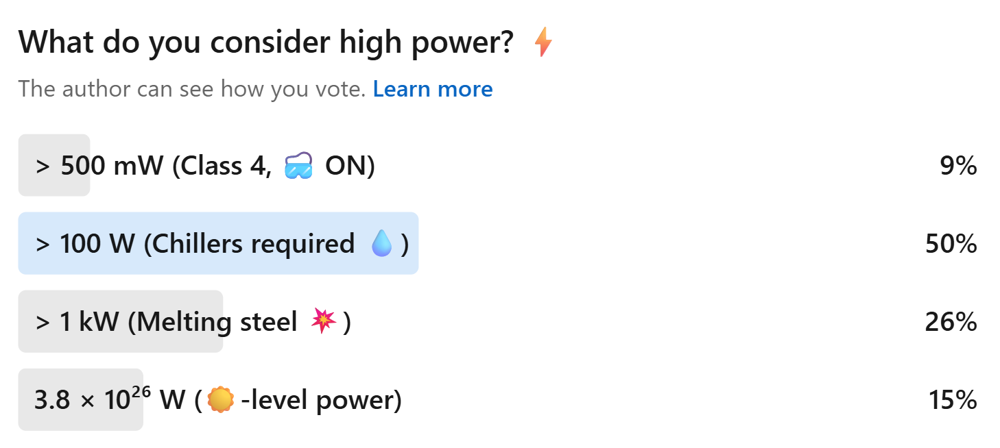
Figure 1. OPTOMAN LinkedIn poll results.
There is currently no universally accepted definition of what is considered a “high-power” in laser optics.
At OPTOMAN, our approach to defining high power in laser optics is centered on Laser-Induced Damage Threshold (LIDT), as it directly reflects the interaction between laser parameters, coating absorption, defect density, and long-term reliability. The ISO standard defines LIDT as “the highest quantity of laser radiation incident upon the optical component for which the extrapolated probability of damage is zero”. LIDT is typically expressed in terms of energy density, power density, or linear power density; it marks the operating point beyond which optical properties such as reflectance or transmittance begin to degrade. When systems operate too close to this threshold, optical properties like reflectance degrade, leading to failure. By analyzing these failure points, we have established approximate operational boundaries in the fs–ps pulse regime, where Ion Beam Sputtering (IBS) becomes a technological necessity.
Figure 2. Operational boundaries for thin-film deposition technologies in high-power laser applications. The Pulsed Regime LIDT Performance map illustrates the fluence threshold (grey line) above which IBS is required to prevent absorption-induced failure, or color-change, highlighting the superior damage resistance of optimized IBS (OPTOMAN SuperHero Power) compared to standard commercial options.

Figure 2.
Figure 2 illustrates the estimated operational boundaries, where IBS performance transitions from beneficial to essential in the Pulsed Regime. The dashed line approximates the operational limit of standard optics in the ultrafast domain. Below this line, legacy technologies such as E-beam or IAD may suffice. Above it, the density and defect control of IBS become critical; the data highlights a significant IBS performance advantage in the fs-ps regime. While standard coatings and cost‑efficient deposition methods such as E‑beam sputtering can achieve higher LIDT values in the nanosecond regime due to lower internal stress in thick stacks, they typically become limited in the femtosecond domain, where LIDT values often remain in the range of 0.2 to 0.5 J/cm². In contrast, OPTOMAN’s optimized SuperHero Power coatings surpass the 1 J/cm² threshold, reaching 1.084 J/cm² at 200 fs, ensuring reliable performance where conventional coatings begin to fail.
LIDT Scaling and Practical Design Implications
When engineering optics for real-world operating conditions, it is essential to acknowledge that LIDT is not a constant parameter. Instead, it depends on a complex interaction of laser characteristics such as pulse duration, repetition rate, beam diameter, wavelength, electric field distribution, angle of incidence, and the operational regime.
In continuous-wave and nanosecond domains, damage is predominantly thermally driven, which means minimizing electric field intensity in high-index layers is critical to reducing absorption induced heating. In contrast, picosecond and femtosecond pulses are governed by electronic damage mechanisms, including avalanche ionization and multiphoton absorption.
While Magnetron Sputtering serves as a robust standard for many high-power CW systems, Ion Beam Sputtering (IBS) offers distinct advantages when pushing the limits of absorption and defect density.
Critically, scaling LIDT across the transition boundary between these regimes is not valid. As the damage mechanism is different for fs, ns pulses, scaling is quite accurate only in proximity. You can scale LIDT from 4 ns to 20 ns, but it might not be accurate from 0.1 to 100ns. At approximately 20 ps, the damage mechanism changes (Figure 3), so it is not possible to use scaling between these two regions.
Figure 3. LIDT scaling behavior across pulse duration regimes. The curve illustrates the non-linear relationship between damage threshold and pulse length. The highlighted “Transition Zone” marks the critical shift from deterministic electronic breakdown mechanisms (in fs/ps regimes) to stochastic thermal effects (in ns regimes), demonstrating why simple scaling laws cannot be accurately applied across this boundary.

Figure 3.
A coating optimized for nanosecond pulses cannot simply be re-rated for femtosecond applications. The cumulative effects of high repetition rates and larger beam sizes also reduce LIDT in practical applications. At ultrafast frequencies above 100 kHz, thermal loading intensifies even with moderate average power, potentially halving the LIDT compared to low-frequency operation. Similarly, increasing beam diameter in nanosecond systems may reduce the damage threshold. Wavelength dependency further complicates matters; a coating rated for 10 J/cm² at 1064 nm may only withstand roughly 5 J/cm² at 532 nm, emphasizing the inverse scaling with photon energy.
The Role of Ion Beam Sputtering
To overcome the challenges of high-power operation and meet the rigorous demands of modern laser systems, sputtering technologies have emerged as the preferred solution for high-performance optics (Read more in our previous whitepaper “Sputtering vs Evaporation”). While Magnetron Sputtering (MS) remains a robust standard for many continuous-wave (CW) applications, and E-Beam evaporation is often sufficient for the nanosecond pulse regime, Ion Beam Sputtering (IBS) provides distinct advantages where minimizing absorption and defect density is critical. IBS exhibits exceptional thermal stability and near-zero absorption, making it the ideal choice for multi-kilowatt CW systems and the rigorous demands of the femtosecond-picosecond pulsed regime.
This technological capability is supported by independent industry benchmarks. Figure 4 illustrates results from the 1077-nm CW Mirror SPIE Laser Damage Competition, which compared the surface temperature rise of various high-reflective coatings under high-power CW irradiation. There is a good correlation between absorption and surface temperature increase, so this information gives a very good indication of which samples have the lowest absorption. The data reveal a big contrast in thermal stability driven by deposition density. The graph, sorted from lowest to highest temperature rise, shows that dense deposition methods, specifically IBS, Magnetron Sputtering, and Plasma-Enhanced Atomic Layer Deposition (PEALD), consistently occupy the lowest temperature tier, with several samples heating by less than 10°C. Conversely, traditional porous coatings produced by E-beam and E-beam IAD exhibit significantly higher heating, indicatinggreater absorption and a higher risk of thermal failure.
Figure 4. Surface temperature rise of high-reflectivity coatings under 1077 nm CW laser irradiation, sorted by performance (low to high temperature). The data highlights the superior thermal stability of IBS technology (left) compared to E-beam and IAD methods (right), which exhibit significantly higher heating and potential for damage due to absorption. Adapted from R. A. Negres et al., “1077-nm, CW mirror thin film damage competition,” Proc. SPIE 12300 (2022) https://doi.org/10.1117/1.OE.57.12.121910.
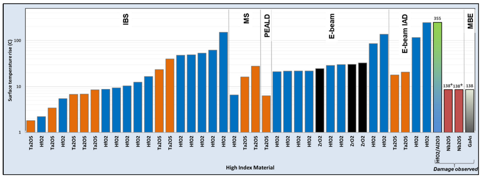
Figure 4.
Beyond thermal stability, sputtering technologies also dominate in ultimate damage resistance. Figure 5 summarizes Ten-years of annual SPIE thin film laser damage competitions since 2008, mapping the “state of the art” across different pulse durations. Historically, porous coatings (IAD/E-beam) held an advantage in the nanosecond regime due to lower stress in thick layers. However, the data confirms that coatings produced by sputtering methods (including IBS) consistently secure the highest damage thresholds in the femtosecond, picosecond, and even CW regimes. This trend is particularly evident in the ultrafast (fs) domain, where the dense, defect-free nature of sputtered films, combined with specific material pairs (e.g., HfO₂/SiO₂), has defined the modern benchmark for ultrafast laser optics.
Figure 5. Winning entries (coating materials and deposition processes) of thin film damage competitions to date as a function of wavelength and pulse length. Christopher J. Stolz, Raluca A. Negres, “Ten-year summary of the Boulder Damage Symposium annual thin filmlaser damage competition,” Opt. Eng. 57(12) 121910 (18 December 2018) https://doi.org/10.1117/1.OE.57.12.121910.
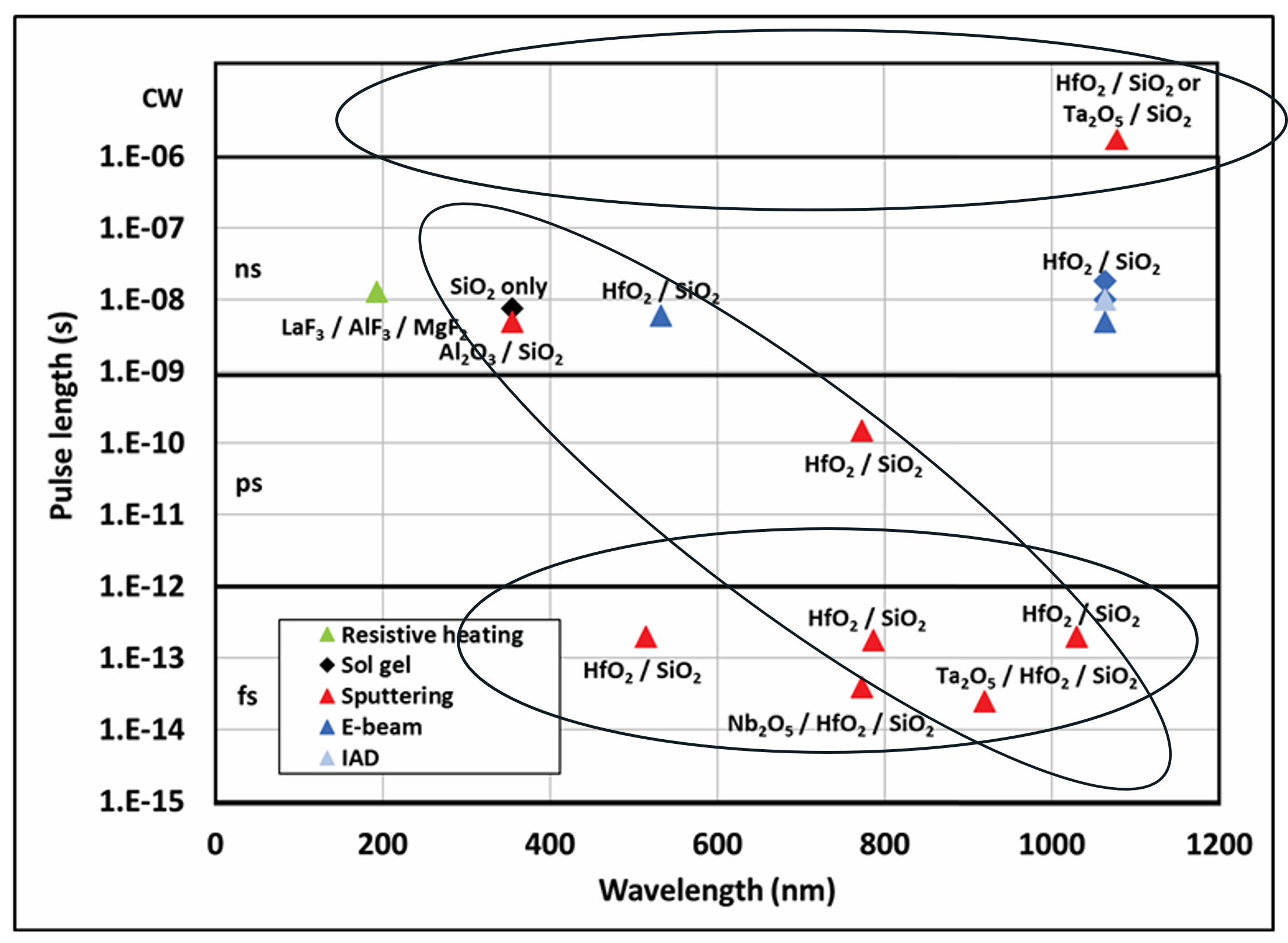
Figure 5.
The New Standard for High Power
It is very difficult to define “high-power” in laser optics, because the demands placed on optical coatings vary dramatically depending on the application. In industrial material processing, high power often means multi-kilowatt outputs, while in display systems or consumer electronics, just a few watts or even milliwatts can qualify. But power alone does not determine the optical component’s survivability. Trying to define high-power optics with a single rule is like using the same map to plan a cross-country road trip and to find your way around your living room; each environment requires its own guidance, shaped by scale, complexity, and purpose.
Because of the different physical processes in the damage mechanisms, no single LIDT value or scaling rule can apply across all regimes. Optics that excel under nanosecond conditions may degrade rapidly under ultrafast pulses, and vice versa. This is why Ion Beam Sputtering (IBS) becomes critical when pushing the boundaries of performance, offering dense, low-absorption, defect-minimized coatings that withstand extreme conditions in both ultrashort pulse and high-power CW applications. Defining high-power optics, therefore, isn’t about setting a single threshold, but understanding the specific regime, application, and failure mechanism, and designing coatings accordingly.