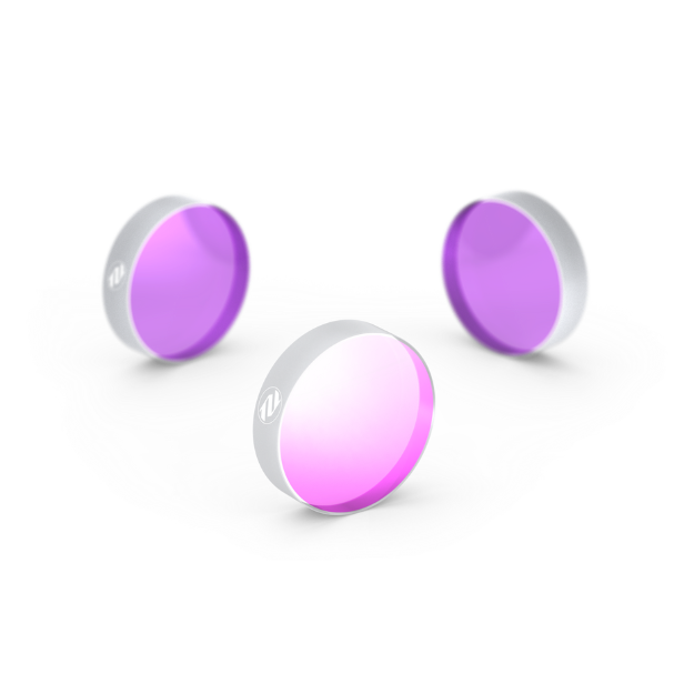
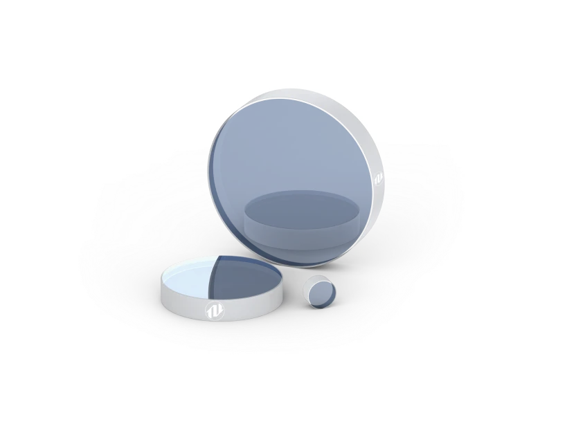
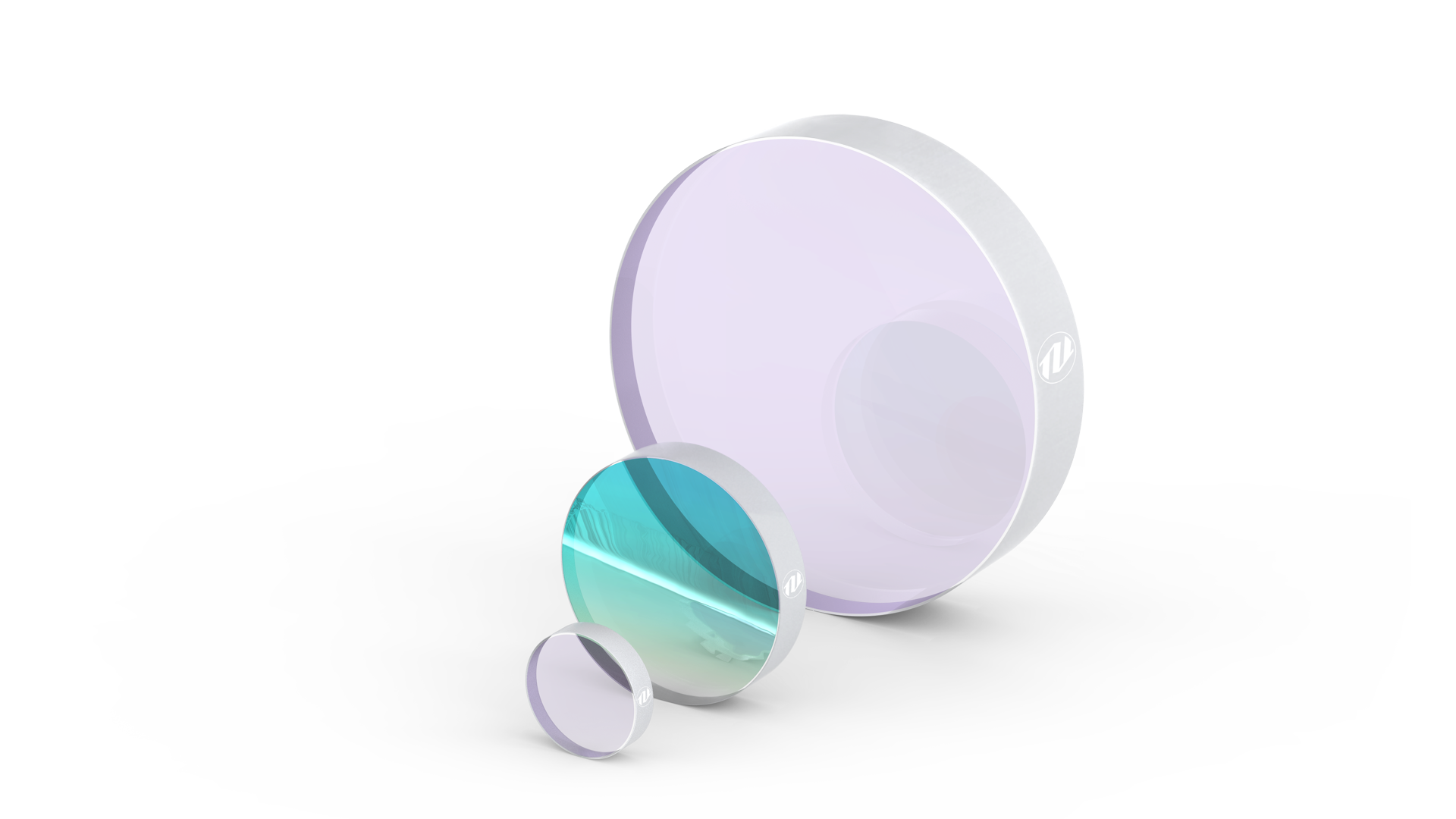
Available Plano Substrates
OPTOMAN has a number of 1/2″, 1″, 2″ and 3” plano substrates in stock, ready to be coated. Choosing the in-stock substrate option allows, on average, saving 6 weeks of lead time and reducing end-product cost 3 times.
Choose the suitable plano substrates and OPTOMAN will make custom coatings on them. OPTOMAN is a coatings superhero, so uncoated substrates are not for sale.
General Specifications
½” substrate (a)
| Material | UVFS |
| Diameter | 12.7 mm (+0/0.1 mm) |
| Thickness | 3.0 mm (+0/0.1 mm) |
| Clear aperture | >90% |
| Surface quality, S1/S2 | 10-5 S-D as per MIL-PRF-13830B |
| Surface flatness, S1/S2 | <λ/10@633 nm |
| Transmitted Wave-front distortion | <λ/10 @ 633 nm over CA |
| Parallelism | <10 arcsec |
| Protective chamfers | 0.1 - 0.2 mm x 45 |
| Chips | <0.1 mm (<0.05 mm best effort |
½” substrate (b)
| Material | UVFS |
| Diameter | 12.7 mm (+0/0.1 mm) |
| Thickness | 6.35 mm (+0/0.1 mm |
| Clear aperture | >90% |
| Surface quality, S1/S2 | 10-5 S-D as per MIL-PRF-13830B |
| Surface flatness, S1/S2 | <λ/10@633 nm |
| Parallelism | <10 arcsec |
| Protective chamfers | 0.1 - 0.4 mm x 45° |
| Chips | <0.2 mm |
1” substrate (a)
| Material | UVFS |
| Diameter | 25.4 mm (+/-0.1 mm) |
| Thickness | 3.0 mm (+/-0.1 mm) |
| Clear aperture | >90% |
| Surface quality, S1/S2 20 | 20-10 S-D as per MIL-PRF-13830B |
| Surface flatness, S1/S2 | <λ/8 @ 633 nm |
| Parallelism | <3 arcmin |
| Protective chamfers 0.2 | 0.2 - 0.4 mm x 45° |
| Chips | <0.2 mm stoned |
1” substrate (b)
| Material | UVFS |
| Diameter | 25.4 mm (+/-0.1 mm) |
| Thickness | 5.0 mm (+/-0.1 mm) |
| Clear aperture | >90% |
| Surface quality, S1/S2 | 10-5 S-D as per MIL-PRF-13830B |
| Surface flatness, S1/S2 | <λ/10 @ 633 nm |
| Parallelism | <10 arcsec |
| Protective chamfers | 0.2 - 0.4 mm x 45° |
| Chips | <0.2 mm |
1” substrate (c)
| Material | UVFS |
| Diameter | 25.4 mm (+/-0.1 mm) |
| Thickness | 6.35 mm (+/-0.1 mm) |
| Clear aperture | >90% |
| Surface quality, S1/S2 | 10-5 S-D as per MIL-PRF-13830B |
| Surface flatness, S1/S2 | <λ/10 @ 633 nm |
| Parallelism | <10 arcsec |
| Protective chamfers | 0.2 - 0.4 mm x 45° |
| Chips | <0.2 mm stoned |
2” substrate (a)
| Material | UVFS |
| Diameter | 50.8 mm (+/-0.1 mm) |
| Thickness | 8.0 mm (+/-0.1 mm) |
| Clear aperture | min 46 mm |
| Surface quality, S1/S2 | 20-10 S-D as per MIL-PRF-13830B |
| Surface flatness, S1/S2 | <λ/10 @ 633 nm per CA |
| Transmitted Wave-front distortion | <λ/10 @ 633 nm over CA |
| Surface irregularity S1/S2 | <λ/10 @ 633 nm per CA |
| Parallelism | <30 arcsec |
| Protective chamfers | 0.4 - 0.6 mm x 45° |
| Chips | <0.1 mm stoned |
2” substrate (b)
| Material | UVFS |
| Diameter | 50.8 mm (+/-0.1 mm) |
| Thickness | 9.52 mm (+/-0.1 mm) |
| Clear aperture | min 45 mm |
| Surface quality, S1 | 20-10 S-D as per MIL-PRF-13830B per CA |
| Roughness (RMS), S1 | <5 ångström |
| Surface quality, S2 | commercial polish (80-50 S-D) |
| Surface flatness, S1 | <λ/10 @ 633 nm per CA |
| Surface irregularity S1 | <λ/10 @ 633 nm over CA |
| Parallelism | <5 arcmin |
| Protective chamfers | 0.2 – 0.3 mm x 45° |
| Chips | <0.3 mm stoned |
3” substrate
| Material | UVFS |
| Diameter | 76.2 mm (+/-0.1 mm) |
| Thickness | 12.7 mm (+/-0.1 mm) |
| Clear aperture | min 61 mm |
| Surface quality, S1/S2 | 20-10 S-D per MIL-PRF-13830B |
| Surface flatness, S1/S2 | <λ/10 @ 633 nm per CA |
| Surface irregularity S1/S2 | <λ/10 @ 633 nm over CA |
| Transmitted Wave-front distortion | <λ/8 @ 633 nm over CA |
| Parallelism | <1 arcmin |
| Protective chamfers | 0.4 - 0.6 mm x 45° |
| Chips | <0.5 mm stoned |
Fill out a custom request
Relax and build your laser. OPTOMAN has your back.

Thank you
for your request
We will contact you as soon as possible