Accelerating Photonics: Emerging Technologies and Startups
The photonics industry is advancing at breakneck speed, pushing the limits of ultrafast material processing, artificial intelligence, and quantum technology. Accelerating Photonics is not just about rapid discovery, but also about translating these advances into practical solutions. But the true test of a superpower isn’t just discovering a new phenomenon; it is engineering that breakthrough into a scalable, rock-solid system that thrives outside the protective bubble of a pristine academic setup. Across the industry, startups and researchers are confronting a common nemesis between academic capability and commercial reliability. Variables that could be endlessly tweaked or forgiven in a lab setup become critical points the moment a system is handed over to an end-user, whether it is operating on a rigorous semiconductor production line or running in an R&D lab.
OPTOMAN is eager to help the next generation of researcher-entrepreneurs cross the commercialization gap.
Startups and researchers aiming to commercialize solutions are of strategic importance to OPTOMAN, as they are shaping the landscape of photonics innovation. Last month at SPIE Photonics Europe, OPTOMAN handpicked three emerging companies to follow and conducted interviews with their founders. We sat down with these leaders to discuss how they are successfully navigating the leap from laboratory prototypes to reliable commercial powerhouses. We spoke with the minds behind RayVen, who are pioneering 2-micron ultrafast lasers to unlock new dimensions in deep-silicon semiconductor processing. Etendue, whose AI-assisted platform is democratizing complex optical design by turning sketches into lightning-fast simulations, and Noisy Labs, which are bringing fragile quantum technology into the real world with portable, room-temperature squeeze lasers. Together, their stories provide a powerful look at how today’s researcher-entrepreneurs are breaking down the barriers between academic brilliance and commercial readiness, proving that the future of photonics extends far beyond the lab.
1. Why 2-Micron Lasers Are the Future
|
Led by dynamic entrepreneur Dr. Célia Millon, RayVen is on a mission to translate academic rigor into cutting-edge industrial solutions. Spun out of the Photonic and Ultrafast Laser Science group at Ruhr University Bochum, RayVen is building a new class of state-of-the-art ultrafast laser systems operating at 2 µm. The company is driven by a bold new vision that this technology will redefine the limits of advanced material processing, environmental monitoring, and scientific research. For researchers, building a cutting-edge laser is a scientific triumph. Taking that laser out of the lab and into the industrial market, however, requires an entirely different kind of engineering. This realization led to the creation of Rayven. After publishing a paper on an 8.7-watt oscillator at 2 microns, the team found themselves fielding calls not only from academics but also from the industrial sector. Initially, the team targeted the academic market. They soon discovered a more lucrative and more demanding application: material processing for semiconductors.
|
Dr. Célia Millon, Founder & CEO, RayVen |

In industry, the reliability threshold is much higher. What matters, maybe even more than performance, is the stability of the laser.
The Superpower of 2 µm
Why the sudden buzz around 2-micron lasers? As RayVen’s founder, Celia explains, it’s not that 2-micron lasers are inherently “superior” to conventional 1-micron systems; rather, they enable processing that 1 µm lasers simply cannot. “You can use 1 micron to process the surface of semiconductors,” Celia clarifies. “But the moment you want to work through or inside the silicon, you need another wavelength.” The demand for processing inside silicon is being driven by the cutting edge of modern electronics, including co-packaged optics, heterogeneous chip integration, and the massive push for 3D stacked chips. These technologies require 3D structures built directly into silicon, glass, and polymers. For processing this versatile mix of materials, 2-micron ultrafast lasers are a powerful tool. RayVen uses a holmium-based crystal to reach a 2.1-micron wavelength. The team originally chose it because it supports both high energy and short pulses. The 2.1 µm wavelength also offers a major practical benefit, as it sits in a transparency region that avoids the high water-vapor absorption seen at slightly shorter wavelengths, such as 1.95 µm thulium.
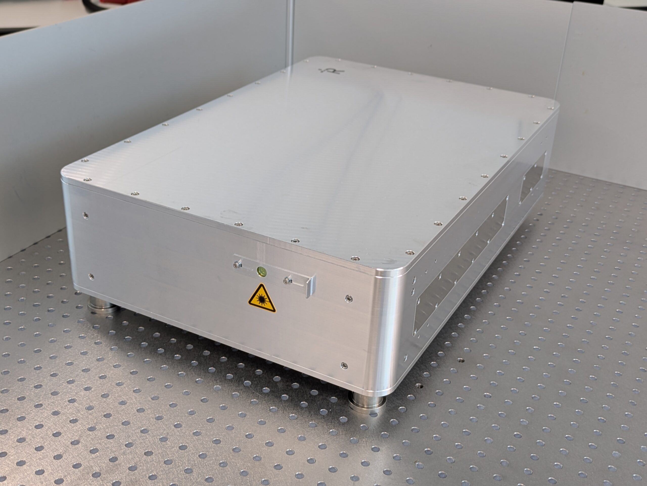
Figure 1. RayVen 2.1 µm ultrafast laser system for advanced material processing applications. |
The Reality of Leaving the Lab
Transitioning from supplying research labs to serving the semiconductor industry comes with harsh realities. The biggest hurdle is reliability. “In research, you have time to try things and see if your components work,” Celia notes. “In industry, the reliability threshold is much higher. What matters, maybe even more than performance, is the stability of the laser.” She points out that building a stable laser is notoriously difficult, and experimenting with new optics or coatings is expensive and time-consuming. In an ideal world, she adds, small startups would have an easier time ordering and testing optics off the shelf, so they could innovate faster.
What’s Next?
While Raven is focused on the semiconductor market, the 2.1-micron ultrafast laser has strong potential in other industries. Each opportunity comes with its own roadblocks:
- Space communication: The 2.1 µm wavelength is advantageous for avoiding water-vapor absorption in the atmosphere. However, the aerospace ecosystem is currently built around 1.5-micron telecom wavelengths, and shifting to 2 microns would require coordinated updates to detectors and LiDAR systems across major players.
- Medical applications: Two-micron continuous-wave lasers are already widely used in medicine. Moving to ultrafast pulses could, in theory, expand options in areas such as lithotripsy (kidney stone removal), ophthalmology, and dermatology. For a young startup, heavy regulatory and certification requirements make the medical sector difficult to enter.
- Research potential: Celia highlights a gap in the research and application of 2-micron ultrafast lasers, particularly in the medical field. Despite 2-micron continuous wave and quasi-continuous wave lasers being widely used in medicine (ophthalmology, lithotripsy, etc.), there hasn’t been sufficient dedicated research to explore the benefits of switching to ultrafast pulses in these applications. Celia mentions that existing publications often compare “pears and carrots,” making it difficult to definitively understand where ultrafast 2-micron lasers could offer a significant advantage, such as in lithotripsy, specific niches of OCT, or certain skin treatments. This indicates an “under-explored field in academia” that could potentially unlock new, more effective medical procedures.
Advice for Researcher-Entrepreneurs
When asked what advice she has for aspiring research entrepreneurs, Célia’s response is surprisingly simple: “It’s not only about the technology.” She points out that while scientific brilliance is essential, it is merely the starting point for everyone in the photonics industry. To turn a great laser into a great business, founders must deliver the whole package, between brilliant physics and real-world business and marketing strategy.
2. AI Breaking Down Barriers in Photonics
|
Thibaut Aitche, The Founder of etendue.io |
Led by innovative founder Thibaut Atché, Etendue is on a mission to democratize optical design and break down the steep barriers of traditional simulation software. Built to serve small and big companies alike, Etendue provides a highly accessible, AI-assisted raytracing platform. Their bold new vision is that simulating complex optical setups should not require months of training or massive budgets, but rather an intuitive, lightning-fast interface that empowers engineers to test and optimize their designs in just a few clicks. Indeed, as powerful as they are, traditional optical design software comes with steep barriers: it can be expensive and notoriously difficult to master, often requiring weeks or even months of training. As a result, many optical projects never see the light of day, as engineers are forced to limit what they explore. The complexity of traditional tools artificially constrains innovation, leaving much of the industry’s optical design potential untapped. A new AI-assisted platform called etendue.io aims to change that by making advanced optical simulations accessible, fast, and easy to use. |

While the user still needs to review the final model, the AI automates roughly 90% of the manual work.
AI Assistant: From Idea to Simulation in Seconds
At its core, Etendue is an optical design platform that applies modern technology to a traditionally rigid field. The platform introduces two major workflow innovations. First, it includes an AI assistant. Instead of manually building a complex setup from scratch, an engineer can feed the AI a PDF, picture, or drawing. The AI reads the file and automatically rebuilds the described optical setup inside the platform. While the user still needs to review the final model, the AI automates roughly 90% of the manual work. Second, the platform uses modern hardware parallelization to accelerate the process. By optimizing how the software uses cloud computing and local hardware, Etendue can shrink simulation times by up to a factor of 1,000.
Tracing the Path of Light
Etendue supports three major modes of light propagation modeling:
- Sequential mode: Accounting for about 90% of use cases, this mode relies on geometry to look only at light that follows a certain, predefined path, tracking it surface after surface. It is the main mode used for smartphone cameras, telescopes, microscopes, and essentially any imaging or beam shaping system.
- Non-sequential mode: Allows light to take multiple, unpredictable paths, which is useful for complex scattering or illumination setups.
- Gaussian mode: Used to represent the physical properties of a laser beam, such as waist size and waist location for niche applications, offering a more physical representation of what happens to a laser beam.
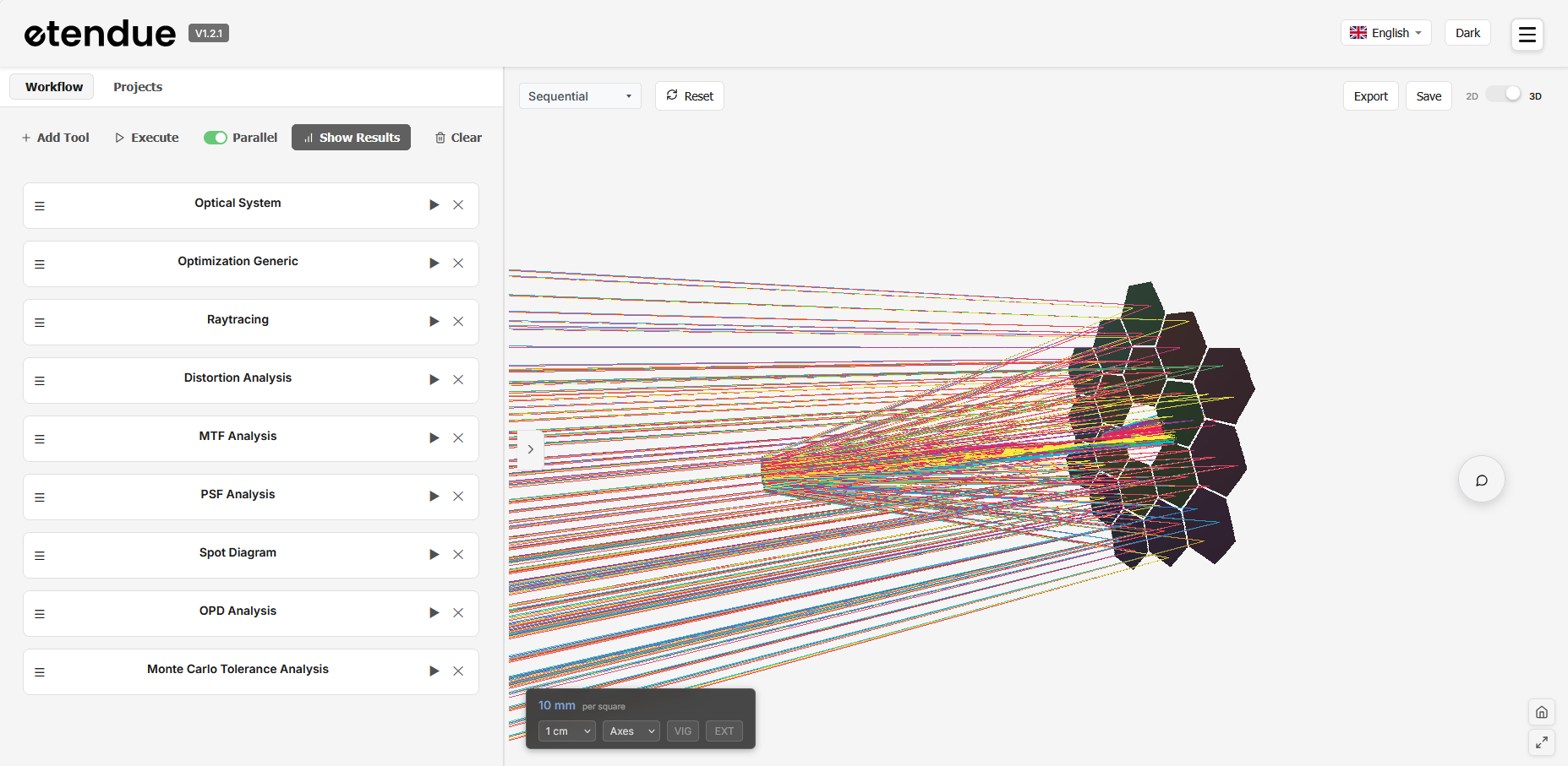
Figure 2. The etendue.io platform interface showing sequential raytracing of a multi-element optical system. The workflow panel on the left lists analysis modules including optimization, distortion analysis, MTF, PSF, and Monte Carlo tolerance analysis.
The Next Frontier: Thermal Effects and Complex Geometries
Optical systems are rapidly evolving. As the guest points out, systems are not necessarily using more elements, but the elements themselves are becoming far more complex. The industry is shifting away from classical lenses toward intricate geometries like aspheres and freeforms. This complexity introduces new challenges, especially when it comes to the gap between computer simulation and real-world performance. Today, some of the hardest phenomena to model accurately are thermal effects and material deformation. When building lightweight systems, such as those required for space exploration, engineers may want to use plastics. A key question is how those plastics will behave under extreme environmental stress or heat. Bridging this gap and using AI to recommend materials that balance optical specifications with environmental durability is a major frontier for optical design software.
What About Data Privacy?
Integrating AI into proprietary engineering designs naturally raises data privacy concerns. Etendue addresses this by separating its cloud and local offerings. The cloud-based version protects user privacy by legal safeguards and does not learn from, or train on, the data that users upload. The offline local version allows all computation and the AI to run and learn securely on the user’s own hardware, thus guaranteeing privacy at the hardware level. By drastically lowering the barrier to entry, Etendue is helping ensure that the future of optical design is not limited to industry giants. It is accessible to any engineer with a great idea and a sketch.
3. Squeezed Light from Noisy Labs for the 2nd Quantum Revolution
|
Noisy Labs is on a mission to accelerate the 2nd quantum revolution. Founded in 2023 with support from the German government’s Exist program, Noisy Labs builds on over a decade of research at the University of Hamburg and University of Hannover. Their vision is to commercialize portable “Squeeze Lasers”, eventually turning fragile lab setups into an accessible, robust tool for next-generation quantum sensing, computing, and communication. For decades, squeezed light technology has been locked behind the doors of academia, requiring massive budgets, controlled conditions, and years of highly specialized training. The team at Noisy Labs is working to change that by turning a research-grade breakthrough into a practical tool that can be used beyond a single, carefully tuned lab setup. |
Dr. Axel Schönbeck, CEO & Co-Founder, Noisy Labs |
The goal is a commercially available squeezed light source that is intuitive enough for someone in a lab to learn to operate it after a single day of training.
Bridging the Quantum Gap
According to CEO and Co-Founder Dr. Axel Schönbeck, Noisy Labs occupies a distinct niche within the quantum technologies ecosystem, engineering squeezed light, a precisely controlled quantum state that reduces noise below the standard quantum limit. This capability sits at the heart of two major application areas: Ultra-sensitive quantum sensing, where lower noise directly translates to better measurements, and quantum computing, where high-quality quantum states are a foundational requirement.
The idea for commercial squeezed light sources traces back to developments made in the gravitational wave detection community. After pushing squeezed-light performance to the limits in this context in academic settings, a growing commercial pull became noticeable: research groups in both the US and EU increasingly wanted accessible squeezed-light sources that were not confined to large scale and fragile laboratory builds.
The Mechanics of Squeezed Light
The term “Squeezed light” refers to an electromagnetic field in which the quantum uncertainty in a specific property (e.g. the phase or amplitude quadrature) is reduced below that of the quantum ground state. That way, a noise suppression of greater than a factor of ten is possible and realized in non-linear crystals using cavity enhanced degenerate parametric down-conversion. This technology allows for the reduction of quantum noise while preserving useful signal information.
Turning that concept into a commercial product is an engineering challenge because the quantum state is sensitive to optical loss and instabilities resulting from changing environmental conditions. Even with those constraints, the Noisy Labs team has managed to build the system using off-the-shelf components, reducing cost and making future scaling more realistic.
Room Temperature and Real-World Readiness
One standout feature of Noisy Labs’ squeeze lasers is that they operate at room temperature, which immediately broadens the range of environments where they can be deployed. Dr. Schönbeck emphasizes that the underlying physics is already well established, the remaining work is focused on translating proven principles into products that can be built, shipped, and supported at scale.
Because these systems are intended for real-world use, they must tolerate variables such as temperature drift and vibrations. To address this, Noisy Labs has prioritized robustness and user-friendliness so that teams can integrate squeezed-light sources into existing setups without requiring deep, highly specialized maintenance expertise.
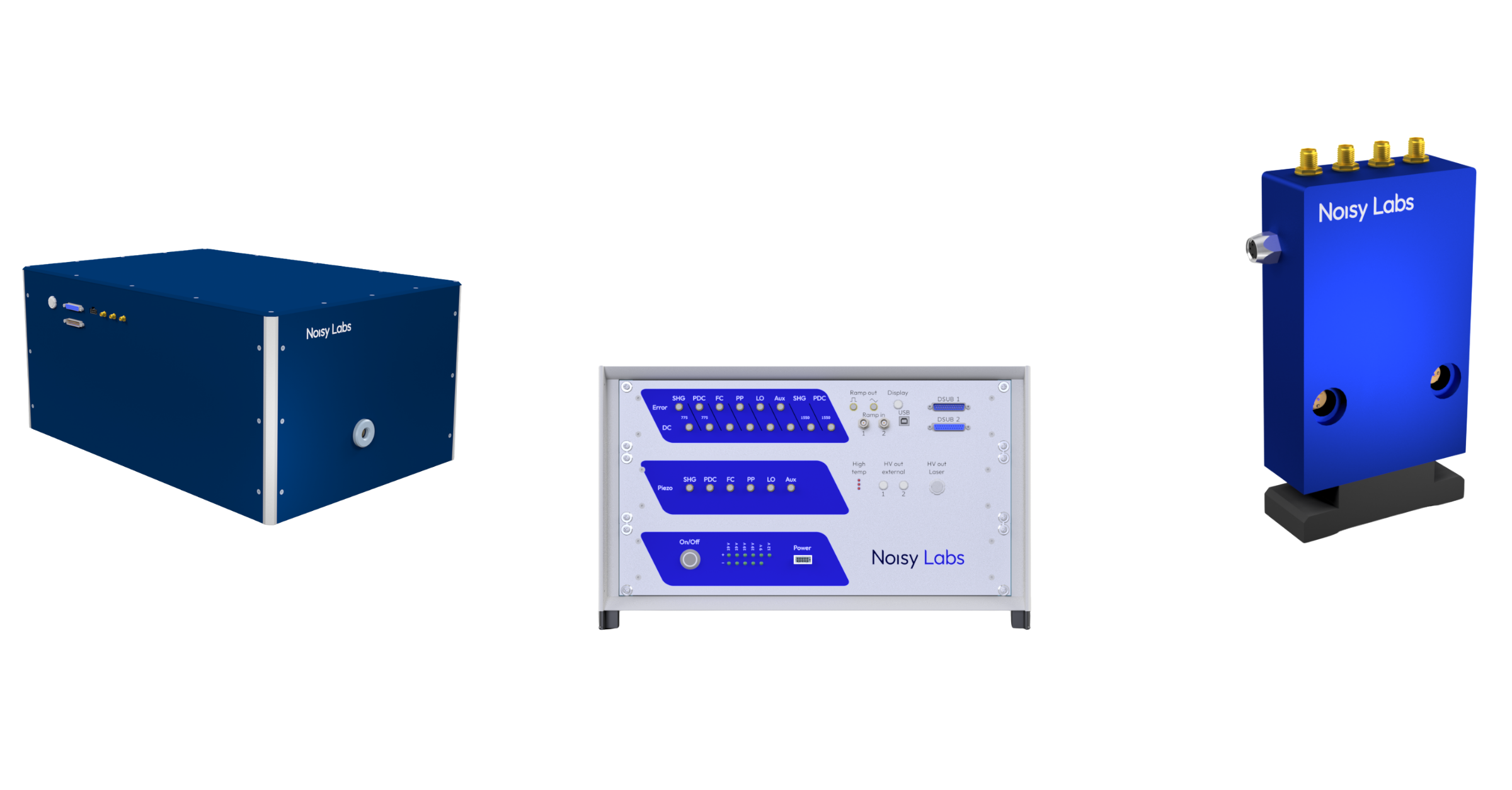
Figure 3. Noisy Labs hardware suite: main enclosure housing the optical and electronic components of the squeeze laser (left); BD-HQE high-quantum-efficiency balanced detector for homodyne detection of squeezed quadratures (center); electronic control rack providing servo control and signal processing (right).
What’s Next: From Sensing to Computing
Where will squeezed lasers make their first major impact? Dr. Schönbeck points to quantum sensing. While it is still a niche today, sensing has clear potential in various applications ranging from biomedical applications to optomechanics and interferometry, where more sensitive measurements can translate into practical advantages. Once the sensing market matures, Noisy Labs plans to extend its squeezed-light sources toward the longer-term ambition of quantum computing. In the company’s view, building the core photonic capability now, with product-grade stability and manufacturability, creates a foundation that can serve multiple quantum applications over time.
Ultimately, the most important innovation may be accessibility. Noisy Labs’ guiding principle is that quantum technology must be easy to use, which means packaging cutting-edge performance into tools that feel familiar to working scientists and engineers. The goal is a commercially available system that is intuitive enough for someone to learn to operate effectively after a single day of training.
The Future of Photonics
As the photonics industry accelerates at an unprecedented pace, the gap between theoretical physics and everyday industrial application is closing faster than ever before. Startups are leading this charge, proving that the future of photonics lies not just in breaking scientific records but in building accessible, reliable systems that can withstand the uncompromising demands of the real world. From deep-silicon semiconductor processing and AI-driven optical design to quantum optics, the technology of tomorrow is rapidly leaving the laboratory behind.
OPTOMAN proudly supports and champions emerging companies, believing that collaboration is key to progress. By engaging with new technologies and innovative startups, we constantly push ourselves to stay at the edge of innovation. Our own journey, guided by founders Remigijus Šliupas and Dr. Simonas Kičas, started with the same entrepreneurial spirit, transforming scientific knowledge into tangible solutions. Having traveled this challenging yet rewarding road ourselves, we deeply appreciate the determination it takes to turn bold ideas into reality. Every new startup pushing the boundaries of what’s possible challenges us to grow alongside them, building the future of photonics based on emerging technologies and collaboration.