
Particle Defects and the Limits of High-Power Laser Optics
The Scaling Demands of High-Power Laser Systems
This article examines the root causes of optical coating failure in high-power laser systems and the manufacturing approach best suited to addressing them, drawing on conversations with leading researchers. The laser industry is undergoing a sustained increase in operating power across virtually every application segment. In industrial material processing, multi-kilowatt continuous wave (CW) systems have become standard. Ultrafast laser systems are pushing into the petawatt regime, and laser-driven fusion programs across the globe are driving requirements for optics at scales and durability levels previously considered hardly reachable. These trends converge on multiple engineering constraints in the optical coating. Substrates can be polished to sub-Angstrom levels, and laser architectures can be refined, but the coating remains the interface where light meets matter, under the highest localized stress in the entire system. The problem is not merely one of material selection, coating thickness, or stress. It is a problem of defects, specifically nanoscale contamination, which is present to some degree in every coating process and determines whether a given optic will fail gradually or catastrophically.
At SPIE Photonics Europe and Optical System Design 2026, we sat down with Andreas Wienke (Laser Zentrum Hannover e.V.), Christian Patzig (Fraunhofer IMWS), and Sven Schröder (Fraunhofer IOF) to discuss where the limits of high-power laser optics currently stand, and what it will take to push them further.
Three Damage Regimes, Three Root Causes
Laser-induced damage in optical coatings is a complex phenomenon based on various physical processes. As discussed in our other whitepaper, “Defining High Power in Laser Optics,” the physical mechanism changes substantially with pulse duration, and misidentifying the operative regime leads to engineering solutions that address the wrong problem. No single LIDT value or scaling rule applies across all pulse regimes, and a coating optimized for nanosecond pulses cannot simply be re-calculated for femtosecond applications (see Figure 1).
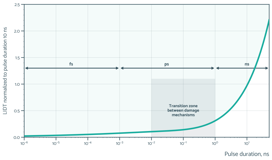 |
Figure 1. Qualitative model of the dominant damage mechanisms vs. pulse duration: particle-driven (ns) and electronic (fs/ps) regimes. The regime boundaries are not sharp; the transition zone extends into the picosecond range, and defects also contribute to damage in the picosecond and CW regimes.
CW Thermal Damage
In continuous-wave (CW) operation, the dominant damage mechanism is thermal rather than electric field-driven. Absorbed power raises the local temperature of the coating and substrate, and damage occurs when the temperature or the temperature gradient exceeds a critical value. Because the process is thermally governed, the CW damage threshold correlates closely with the coating’s absorption and the substrate’s thermal conductivity: reducing absorption and improving heat dissipation both raise the damage threshold [1]. Keeping absorption low is therefore central to reliable high-average-power operation.
Coating microstructure has a direct influence here. Porous films can absorb atmospheric moisture, increasing absorption and causing the spectral response to drift with temperature and humidity. These effects become limiting as average power rises. Ion beam sputtering (IBS) produces fully densified, near-bulk-density films with correspondingly low absorption and high thermal and spectral stability, making it well suited to multi-kilowatt CW systems.
Nanosecond Particle-Driven Damage
In the nanosecond regime, the failure mechanism shifts from thermal to particle-driven. Absorbing microparticles act as localized hot spots: if the energy deposited by a nanosecond pulse exceeds their damage threshold before thermal diffusion can provide relief, it will result in explosive ejection and catastrophic damage. Particle density and the particles’ damage threshold become the limiting specifications, rather than the bulk properties of the coating material.
“In my opinion, nanosecond damage is mainly particle-driven. Particles lead to catastrophic damage quite easily.” — Christian Patzig, Fraunhofer IMWS
“The main constraint of ns-LIDT is that everything comes down to defects. Even single defects can lead to a complete fallout of the optic. Even in a cleanroom, defects are generated unless you work in a high-level semiconductor environment. ” — Andreas Wienke, Laser Zentrum Hannover
Ultrafast Electronic Damage
In the femtosecond and short-picosecond regime, damage is initiated primarily through multiphoton and avalanche (impact) ionization, and the single-pulse threshold scales with the electronic bandgap of the coating materials. Unlike the nanosecond regime, where damage is statistical in nature, driven by defects and inclusions, breakdown in the ultrafast regime follows deterministic scaling laws, with the threshold fluence varying systematically with bandgap and pulse duration (the Mero–Rudolph scaling) [2]. Because the two regimes are governed by different physics, nanosecond scaling laws cannot simply be extended across the transition, which occurs at only a few picoseconds, short-pulse behavior must be described by its own model.
Below the catastrophic threshold, coating layers can also undergo density changes that are detectable as a spectral shift, a “color-change” effect. It is not always clear whether this represents a distinct failure mode or an early onset of the same multiphoton absorption that leads to catastrophic damage once the fluence is raised slightly. Its behavior under repeated irradiation is likewise variable: in some cases, the accumulated change produces long-term fatigue that gradually degrades the optic, while in others it stabilizes with no further effect.
“Ultra-short pulses have a different damage mechanism, one that is more electronic in nature. And morphologies are completely different, really quite unlike what we see in other regimes.” — Christian Patzig, Fraunhofer IMWS
“Whether a color change already constitutes damage when the optic is still performing as it should is a question the standardization community is actively working on. It is currently implemented into the next revision of the ISO standard.” — Andreas Wienke, Laser Zentrum Hannover
The Physics of Particle-Initiated Failure in Detail
Understanding why particles are so damaging in the nanosecond regime requires examining what happens at the defect site on the relevant timescales. A particle embedded in a dielectric coating stack has different optical and thermal properties than the surrounding coating material. When a nanosecond pulse passes through, the particle absorbs a disproportionate fraction of the incident energy either because it has higher intrinsic absorption or because it creates a local field enhancement in the coating’s standing-wave pattern. Because heat diffusion into the surrounding dielectric is slow relative to the pulse duration, the particle reaches extreme temperatures before energy can be dissipated, resulting in thermal expansion, phase transitions, and ultimately explosive ejection, which creates a damage crater that nucleates further failure on subsequent pulses (see Figure 2).
Identifying the root cause of damage at a site locally requires cross-sectional analysis. Damage sites that look similar under light microscopy can reveal fundamentally different failure modes when examined in cross-section by focused ion beam (FIB) milling followed by scanning or transmission electron microscopy (SEM and TEM). These high-resolution methods resolve the damage morphology in detail and allow conclusions to be drawn about its underlying cause.
Such analyses are too time- and cost-intensive to form part of every standard measurement, so their role lies in dedicated failure analysis rather than routine testing. Where they are applied, they offer a level of causal insight that was previously unavailable, particularly in the nanosecond regime, where identifying the causes of damage has traditionally relied more on empirical observation.
“If you cut the damage site open with the focused ion beam machine and really look at the cross-section, you can see it might have been a particle. We have seen this lots of times, but it might also have been a kind of delamination between the coatings where you have some weak interfaces. What we also found on many IBS coating systems is a visible bubble formation on the nm scale, what we interpret as local accumulation of the process gas, especially if it was Ar, entrapped within the layer stack, usually within the high-index layers. The deeper you look, the more you find.” — Christian Patzig, Fraunhofer IMWS
The argon bubble finding is directly relevant to optimizing the IBS process. Trapped working gas creates localized low-density regions that behave analogously to extrinsic particles, initiating damage below the intrinsic material threshold. Managing gas incorporation is therefore a direct driver of LIDT performance, not merely a process quality concern.
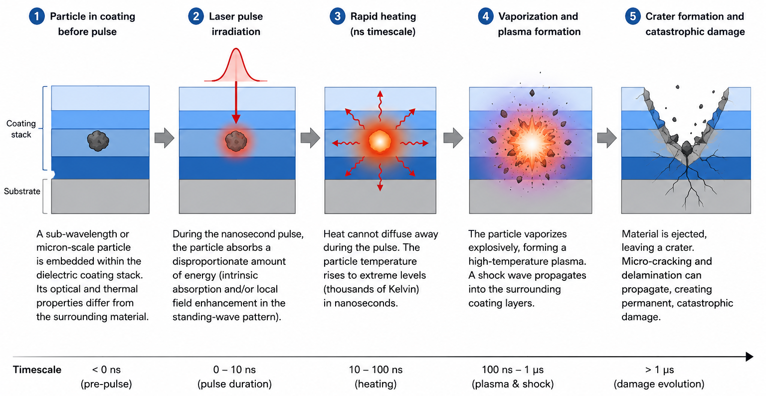 |
Figure 2. Cross-sectional schematic (illustrative diagram, not experimental data) of particle-initiated failure in a dielectric coating stack under a nanosecond pulse.
Why IBS Is the Appropriate Response
IBS addresses the particle problem through a process architecture that is fundamentally different from alternative deposition methods. The target and substrate are physically separated, with material ejected by a precisely controlled ion beam using ultra-high-purity target materials. The system operates at a low base pressure (typically around 10⁻⁶–10⁻⁷ mbar), with a process pressure of approximately 10⁻⁴ mbar during deposition. The spatial separation between the sputtering and deposition zones (see Figure 3) significantly reduces the likelihood of contamination reaching the substrate, thereby producing coating layers with near-bulk packing density and minimal working-gas entrapment.
The bulk-like density also eliminates water absorption, a failure pathway in porous e-beam coatings that causes spectral drift and elevated absorption under varying humidity conditions. IBS coatings, being fully densified and amorphous, are immune to this effect. Under optimized IBS conditions, total absorption values below 1 ppm of a HR mirror at 1064 nm are achievable, reflecting end-to-end process control across substrate preparation, chamber cleanliness, target purity, and post-deposition handling. OPTOMAN’s specialization in IBS allows process parameters to be optimized in ways that generalist operations cannot match. Every coating run and every quality failure feeds back into one technology platform, building cumulative mastery of the variables that translate directly into lower defect density.
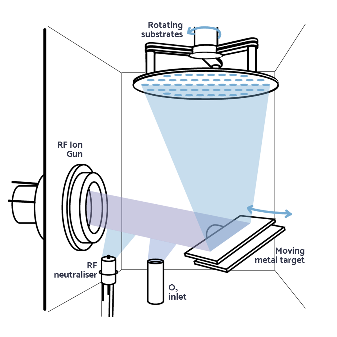 |
Figure 3. Ion Beam Sputtering geometry: spatial separation of target and substrate in a high-vacuum chamber.
The Fusion Demand: Scaling the Challenge
Laser fusion programs represent the most demanding convergence of the challenges described above. Systems targeting commercial power generation require optics that operate at high-nanosecond fluence, scale to 400-mm apertures, and maintain performance over years, all within a cost structure compatible with eventual commercialization (see Figure 4).
“The main constraint for the operation of a laser fusion power plant is always the LIDT of the optics. If the optic breaks, the fusion power plant gets less efficient. Pushing these limits is still a challenge, and that is what makes it interesting for us.” — Andreas Wienke, Laser Zentrum Hannover
The NIF model of continuous optic refurbishment is explicitly not the target for European commercial fusion programs. The requirement is durability, which makes particle-driven damage an existential engineering problem: a coating that fails due to particle initiation below the intrinsic threshold cannot be fixed by simply scaling up the aperture.
“There are approaches where they go for femtosecond pulses close to the chamber, but basically all beamlines will have nanosecond pulses and high power in the IR. Optics for both IR and UV are necessary.” — Sven Schröder, Fraunhofer IOF
The wavelength landscape adds further complexity. Inertial fusion reactors based on Nd:glass, such as NIF, operate at the fundamental wavelength of 1053 nm, but frequency-conversion stages up-convert the energy to 527 nm (second harmonic) and 351 nm (third harmonic), each imposing different material requirements and LIDT behavior. Shorter wavelengths increase photon energy and lower the threshold for particle-initiated damage, compounding the challenge at every stage downstream of the gain medium.
 |
Figure 4. National Ignition Facility’s laser bays, which have two clusters of 48 beamlines. Credit: https://lasers.llnl.gov/
Metrology as a Co-Requirement
The ability to distinguish between intrinsic material damage and particle-initiated failure is crucial for process improvement and requires a layered characterization approach.
“Every ppm counts in certain optical systems. It is not just the LIDT. We expect that at some point a simple LIDT value is not enough anymore to specify laser stability” — Sven Schröder, Fraunhofer IOF
This points to a broader shift in how the industry thinks about optical quality. A single LIDT value, measured at a single pulse duration and wavelength, captures only one failure mode under one set of conditions. It says nothing about how the coating behaves under sustained average power, how its damage threshold evolves over millions of pulses, or whether a given damage event was initiated by an intrinsic material limit or by a single sub-micron particle that happened to fall within the beam. As power densities increase and operational lifetimes extend into the gigashot regime, specifying an optic by LIDT alone is equivalent to specifying a structural material by its tensile strength without measuring fatigue, fracture toughness, or corrosion resistance. The number is real, but it is incomplete.
As illustrated in Figure 5, a complete characterization stack moves from surface-level metrics toward progressively deeper diagnostic insight. Absorption measurement at the ppm level, using photothermal techniques such as laser-induced deflection or laser calorimetry, provides the key process metric for CW and nanosecond performance. LIDT testing under standardized protocols, S-on-1 for fatigue-sensitive applications and raster scan for area statistics, provides damage threshold data. Angle-resolved and total light scattering measurements analyze scattering behavior and scattering losses down to sub-ppm levels, providing insight into surface and coating imperfections. At the deepest level, FIB-SEM cross-sectional analysis, as applied by research institutions such as Fraunhofer IMWS, provides failure-mode identification that optical inspection cannot achieve, revealing whether damage originated from a particle, a weak interface, or a gas-related defect within the coating stack.
OPTOMAN’s metrology approach relies on independent verification through LIDARIS. This provides access to calibrated, standardized testing under well-documented protocols, a critical factor given the ongoing disputes within the laser optics community over measurement methodology and reported damage threshold values.
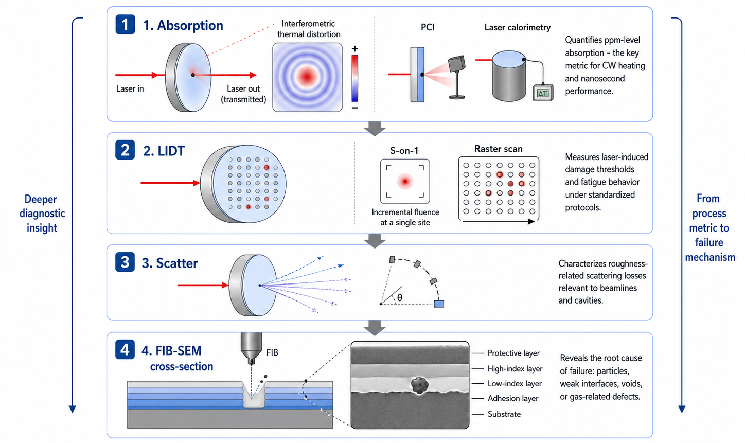 |
Figure 5. Layered metrology stack: absorption (PCI / calorimetry), LIDT (S-on-1, raster), scatter, and FIB-SEM cross-section.
Conclusion
In nanosecond-pulsed high-power laser systems, particle contamination is the dominant cause of optical coating failure. It operates below the intrinsic material threshold and cannot be solved by material selection alone. It requires process control at every stage of deposition. IBS is the method best suited to that requirement, and the same platform addresses the electronic damage mechanisms and color-change degradation that define the ultrafast regime. Two distinct physical problems, one manufacturing solution.
As laser powers increase and durability requirements extend from months to years, the tolerance for particle-driven failure narrows, and standard coating technologies are not engineered to operate at this level. OPTOMAN’s IBS platform directly addresses each of the failure modes described in this article: near-bulk density that suppresses absorption and thermal lensing, limiting CW optics; minimal particle and working-gas incorporation that raises the nanosecond damage threshold; and advanced layer control for the architectures that ultrafast and color-change-sensitive applications demand. The researchers we spoke with see this not as a limitation but as the definition of the field right now:
“The demands are so high that they push the performance limits of the coatings, and at the same time push the limits of our knowledge about them.”
The author would like to thank Andreas Wienke (Laser Zentrum Hannover), Christian Patzig (Fraunhofer IMWS, Halle), and Sven Schröder (Fraunhofer IOF, Jena) for their time and their candid discussion at SPIE Photonics Europe and Optical System Design 2026, which substantially informed this article.
[1] Kevin Kiedrowski, Marco Jupé, Henrik Ehlers, Michael Kennedy, Andreas Wienke, and Detlev Ristau, “Challenges in the development of a reliable cw-LIDT measurement routine,” Opt. Mater. Express 13, 1712-1725 (2023)
[2] M. Mero, J. Liu, W. Rudolph, D. Ristau, and K. Starke, “Scaling laws of femtosecond laser pulse-induced breakdown in oxide films,” Phys. Rev. B 71, 115109 (2005).