
Efficient Laser Ablation
Ultrafast lasers remove material with a precision that few other tools can match. Femtosecond and picosecond pulses ablate metals, semiconductors, glass, and polymers with little melting, which makes them the tool of choice for drilling, cutting, mold milling, and surface texturing in electronics, medical devices, and tooling. However, this method is limited by efficiency. Ultrafast pulses remove material in very small portions, and the laser power that does the work is expensive. Researchers in Vilnius summarized the problem in 2009: processing quality already met industrial demands, but processing speed was still far from economical industrial use [1]. Average laser power has grown from watts to kilowatts since then, yet the central question remains the same: how much material can each watt remove?
In September 2026, at COLA 2026, the International Conference on Laser Ablation in Vilnius, we spoke with Dr. Mindaugas Gedvilas, Chief Researcher at the Department of Laser Technologies of the Center for Physical Sciences and Technology (FTMC) in Vilnius, about his perspective on this technology.
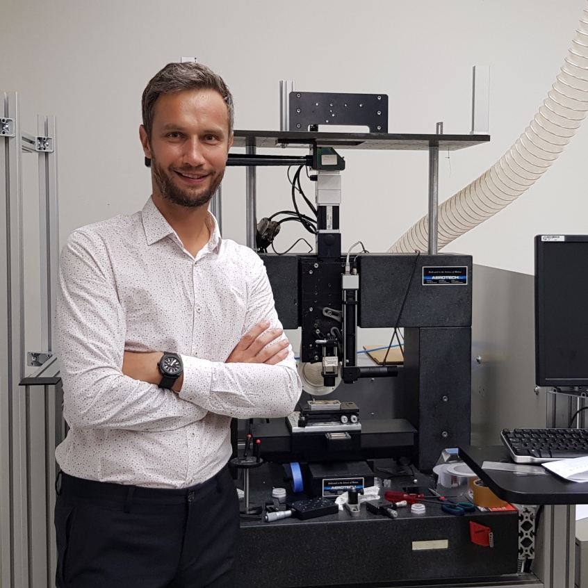
Dr. Mindaugas Gedvilas
Chief Researcher, Department of Laser Technologies, Center for Physical Sciences and Technology (FTMC), Vilnius
Improving Ablation efficiency
For Mindaugas, the most important figure when tracking progress is the volume of material removed per unit of laser energy:
Optical coatings are made to withstand ever higher laser power, so coating makers try to make the laser-induced damage threshold as high as possible. We do the opposite. We try to damage the material as easily as possible and evaporate it as quickly as possible. Our goal is to remove as much material as possible, using as few watts as possible.
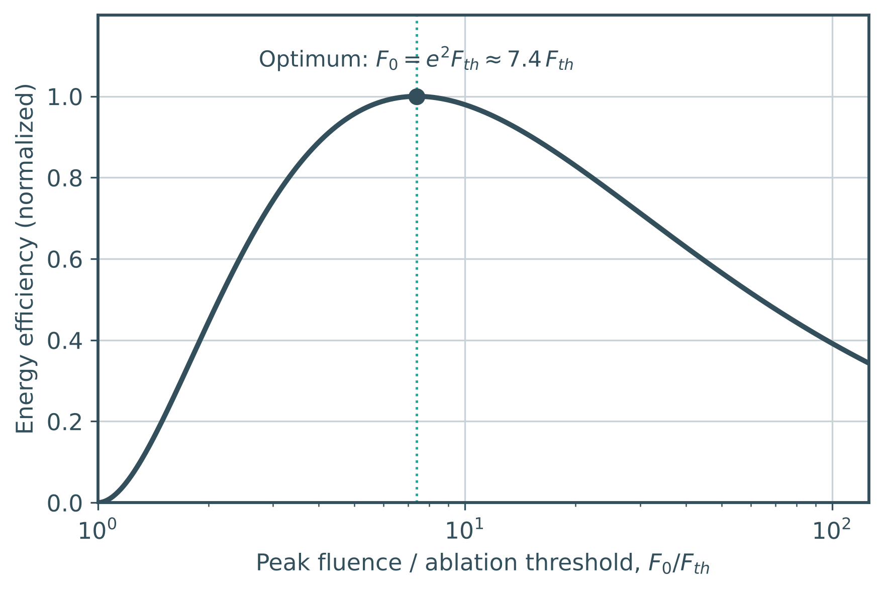
This way, scientists working on laser processing and RnD teams work hand in hand. Ablation starts only above a threshold fluence, and the depth removed by each pulse grows only slowly as the fluence rises. Each joule therefore removes the most material at an optimal fluence of roughly seven times the threshold (Figure 1) [1]. Below the optimum, much of the beam lies below threshold: it heats the material but removes nothing. Above it, each additional joule removes less material, and the surplus energy heats the workpiece and creates an ablation plume, reducing precision through melting and plasma shielding [1].
 |
|
Figure 1. Energy efficiency of ablation (volume removed per unit pulse energy) for a Gaussian beam as a function of peak fluence, normalized to its maximum. OPTOMAN chart based on the logarithmic ablation model [1].
Above a material-dependent fluence, energetic efficiency fell, which the authors attributed to plasma forming above the surface and shielding it from subsequent light. Therefore, raising the pulse energy is an inefficient way to speed up ablation. The optimal spot also grows too large for 1-2 µm features, so the authors proposed splitting high-energy beams into several beams, or removing the bulk with a large spot first and finishing with a small one [1].
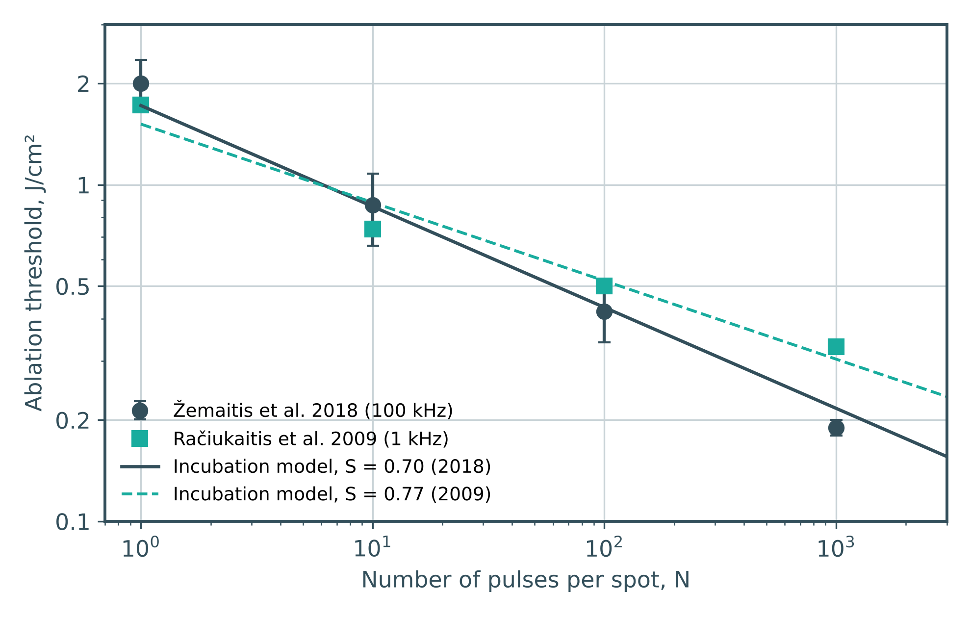
A single pulse below the threshold removes nothing, but it leaves defects that make the next pulse more effective. For copper irradiated with 10 ps pulses at 1064 nm, the threshold falls from 2.0 J/cm² for one pulse to 0.19 J/cm² for 1000 pulses, giving an incubation coefficient S = 0.70 (Figure 2). However, the effect saturates after about 1000 pulses per spot [2].
 |
|
Figure 2. Multi-pulse ablation threshold of copper for 10 ps pulses at 1064 nm. OPTOMAN chart, data from Žemaitis et al. (2018) [2], including the values reported by Račiukaitis et al. (2019) [1].
In practice, the scanning speed and repetition rate set how many pulses hit each spot. In 2018, Gedvilas and co-authors published a scanning model that accounts for both incubation and saturation, helping to choose these parameters for efficient milling [2].
BURSTS: USING THE HEAT INSTEAD OF LOSING IT
Asked about the most important change in his field over the past decade, Mindaugas points to bursts: groups of closely spaced sub-pulses delivered in place of a single pulse. He says bursts have been shown to raise the removal rate by more than ten times, and major conferences now hold dedicated sessions on them. He explains the physics with a comparison:
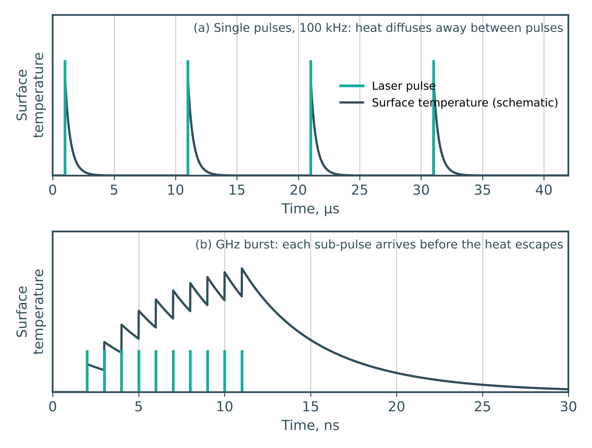
When you fire into the same material again after some time, you are not firing into cold material. With bursts, the next pulse comes so quickly that the heat has no time to diffuse out of the material. You fire the next sub-pulse where the material is still very hot, and you use that heating to remove more material than usual. In a way, you trick nature.”
With single pulses, part of the absorbed energy evaporates material and carries it away, while the rest diffuses into the workpiece and is lost before the next pulse arrives. Inside a burst, the sub-pulses follow each other faster than the heat can diffuse (Figure 3).
 |
|
Figure 3. Schematic surface temperature under (a) single pulses at 100 kHz and (b) a GHz burst of sub-pulses. Inside the burst, each sub-pulse arrives before the heat from the previous one has diffused away.
The gain is easy to see in copper: with the same energy, a GHz burst removed about 600 µm³ of material, almost twice the 330 µm³ removed by an optimized single pulse. New uses are still being found. In 2024, Mindaugas’s group used bursts to mill metal cavities at 13 mm³/min and then polish them, producing moulds for LED diffusers [3]. Still, a faster laser alone is not enough. Mindaugas recalls that when MHz lasers first appeared, higher repetition rates mostly overheated metals and spoiled the quality. Bursts solved this, but each process still needs tuning for every material and laser.
FUTURE PROSPECTS
Much of Gedvilas’s work focuses on functional surfaces: hydrophilic and hydrophobic metals, superhydrophobic textures, and absorbing and optical structures. Shark skin is his favorite example. Under a scanning electron microscope, its rough surface shows small scales that help the skin slide through water more easily than a smooth surface would. Riblet films inspired by shark skin already fly on commercial aircraft: Lufthansa Technik and BASF report fuel savings of about one percent on the Boeing 777 [4]. Lasers can write such structures directly, in almost any shape, but area remains the limit:
In the laboratory you work with small areas. But when you want to make a demonstrator, say five by five centimetres, which is not much, you see that it takes an hour.
Covering a car or an aircraft wing in this way is still out of reach. One route is to laser-machine a stamp once, over an hour or two, and replicate its surface millions of times. The other is a combination of efficient scanning, bursts, and higher average power, as described above. Mindaugas says it would be interesting to test laser-made shark skin structures and study their aerodynamics. Optics is another field for laser structuring. Laser-made nanospike structures on glass act as anti-reflective surfaces through a refractive-index gradient, without any coating [5]. Their weakness is durability: a finger touch or careless cleaning can break the structures. For Gedvilas, solving this would be the breakthrough to wait for:
It would be great to solve the durability problems and make the nanospike structures more resistant, so that we could protect household glass, lenses or safety glasses with them.
The Role of Optics
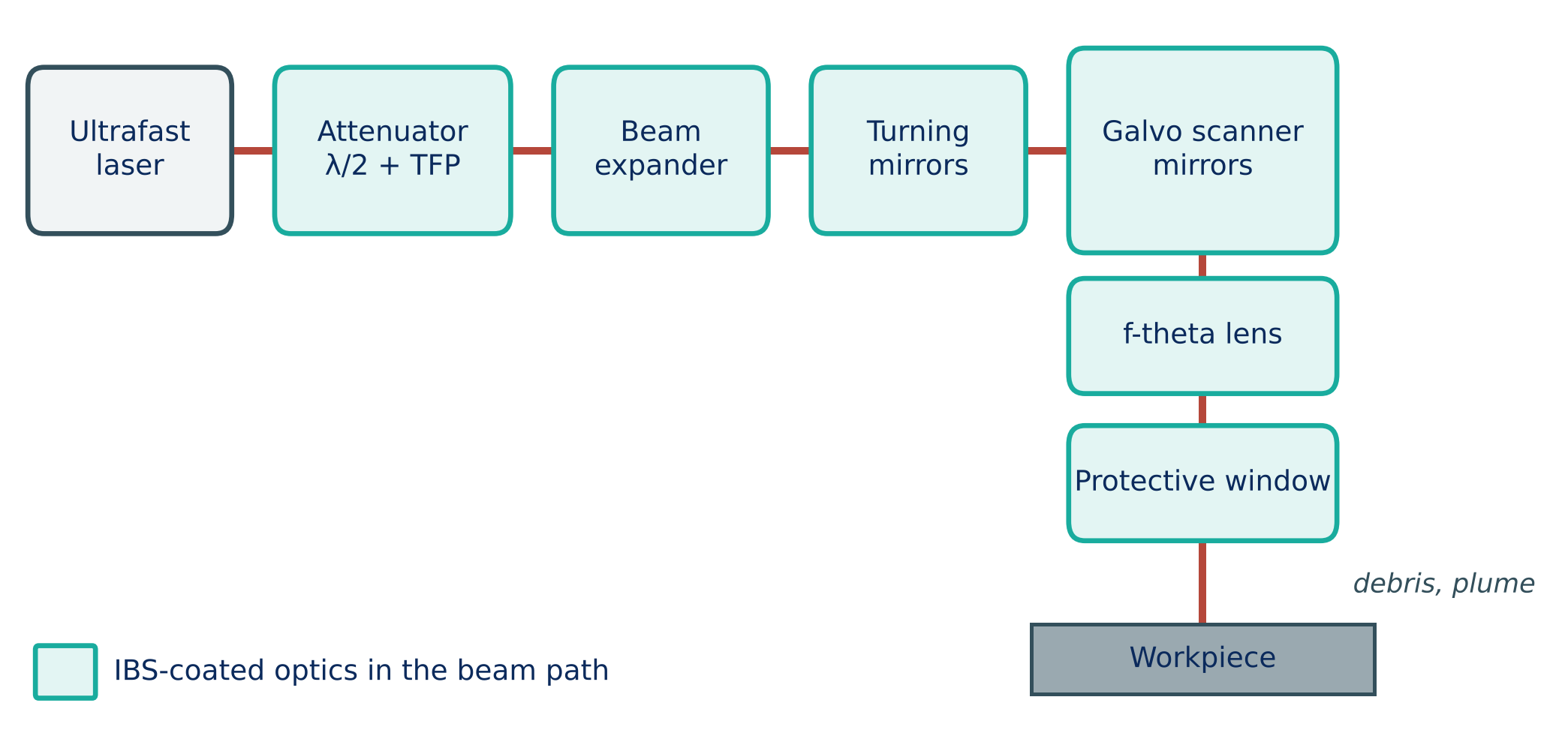
To make laser ablation more efficient, scientists try to remove as much material as possible with every watt of laser power. The optics that deliver the energy must therefore do so with as little optical loss as possible. Every watt absorbed or scattered between the laser and the workpiece is a watt that removes no material, and at hundreds of watts to kilowatts of average power, even small absorption heats an optic, deforms its surface, and shifts the focus. A focal shift changes the spot size and, with it, the F0/Fth ratio that efficiency depends on. Figure 4 shows where coated optics sit in a typical ultrafast processing head.
 |
|
Figure 4. Simplified beam path of an ultrafast laser processing system.
Scanning mirrors for wide angles and high power
Galvanometer scanners place the pulses on the workpiece, and their mirrors see the full average power over a range of angles. Dielectric mirrors reach high reflectivity with low absorption, but only within a limited angular and spectral range, and the thick stacks needed to widen it compromise surface flatness. Metallic mirrors reflect over wide angles, but absorb more. OPTOMAN’s hybrid scanning mirrors combine an IBS dielectric stack with an underlying metallic layer on fused silica, silicon, or silicon carbide substrates. The coating maintains reflectivity above 99.9% from 1060 to 1080 nm and above 99.85% at 1030 nm across 35° to 55° angles of incidence, while reflecting above 90% from 550 to 3000 nm, supporting visible and infrared wavelengths for cameras and process monitoring (Figure 5).
Ru(1060 nm-1080 nm) >99.9% Ru(1030 nm) > 99.85% Ru(550 nm-3000 nm) > 90%; AOI = 35-55°
|
|
|
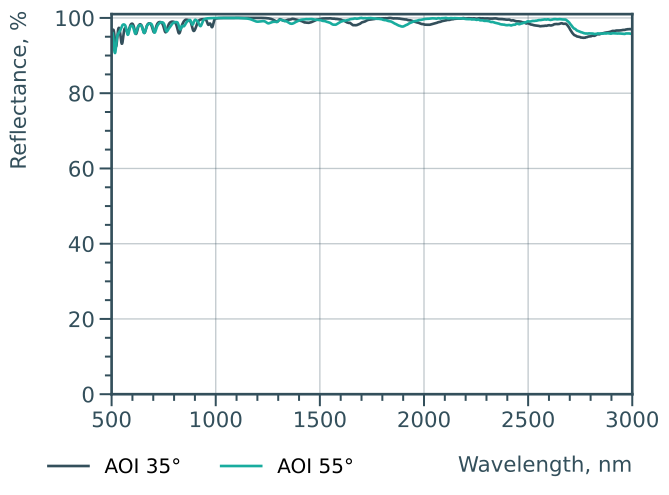
Figure 5. Measured reflectance of the OPTOMAN hybrid scanning mirror coating at 35° and 55° AOI.
At 1070 nm, the median front-surface absorption measured at 35° AOI is 29.45 ppm, and in a 30 s-on-1 test at 36° AOI the coating withstood irradiance up to 19.3 MW/cm² (Figure 6).
a)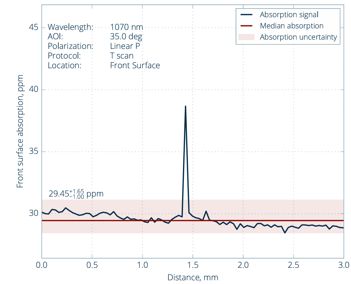 |
b)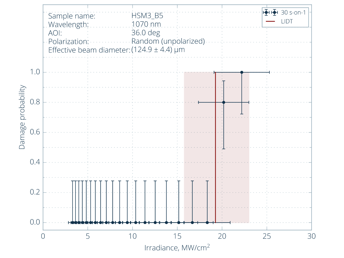 |
Figure 6. Absorption (a) and laser-induced damage threshold (b) of the hybrid scanning mirror coating at 1070 nm.
Protective windows against debris
Ablation throws debris and vapor toward the focusing optics, so a protective window sits between the f-theta lens and the workpiece and is cleaned or replaced as part of maintenance. Because it is the last optic before the process, any absorption turns into a thermal lens that shifts focus. OPTOMAN’s low-absorption protective windows combine IBS anti-reflection coatings with absorption below 3 ppm, a controlled Z-shift, and residual reflectance below 0.1% at 1060–1070 nm and below 2% at the 633 nm alignment wavelength. The coating has been tested above 426 kW/cm² at 1070 nm, and windows are available in 500 mm diameter or 500 × 200 mm sizes.
Non-degrading optics for ultrafast and UV processing
Ultrafast mirrors in a processing machine receive trillions of pulses over their service life, and the gradual threat is not catastrophic damage but fatigue: a color change of the coating that reduces performance long before the damage threshold is reached. OPTOMAN’s non-degrading ultrafast optics withstand more than 0.7 J/cm² at 1030 nm and around 200 fs, with a damage threshold that stays constant from 10 to 10⁵ pulses per site (Figure 7a). The coatings are rated for more than 3.6 × 10¹² pulses at 100 kHz, about 10,000 hours of operation, without color change. For processes run at the harmonics, non-degrading UV mirrors cover 257 to 343 nm and, according to lifetime extrapolation, withstand 0.35 J/cm² without color change for more than 10,000 hours of operation (Figure 7b).
a)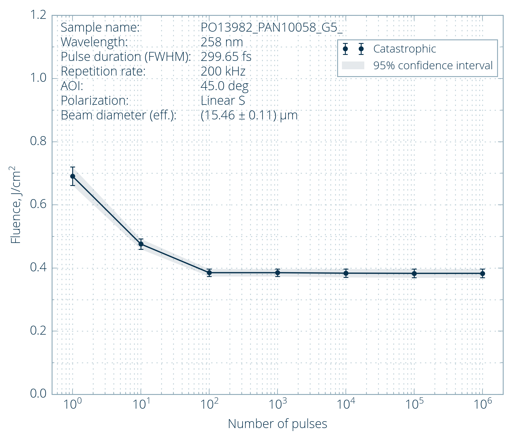 |
|
b)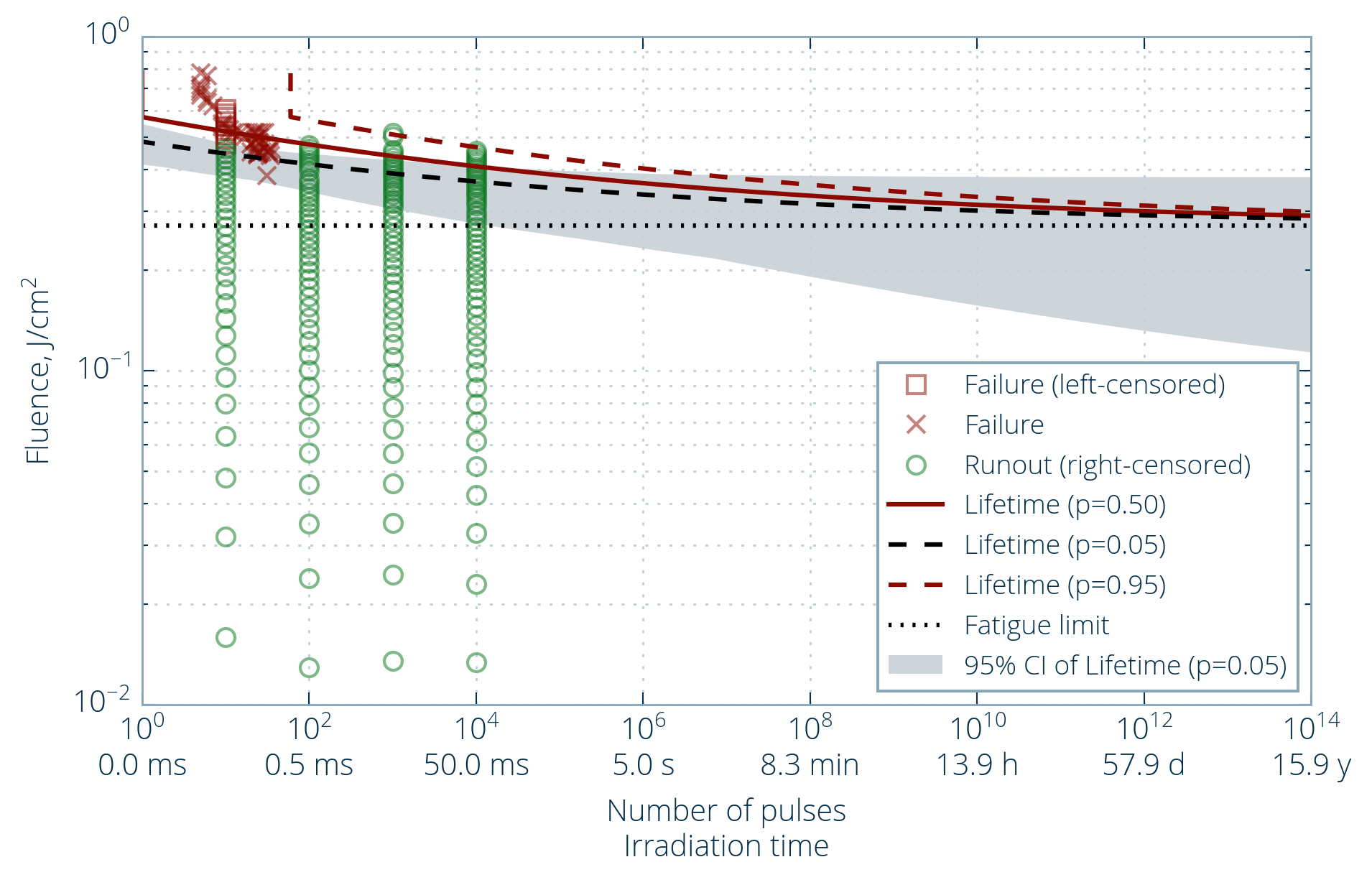 |
Figure 7. Characteristic damage measurement curve of a highly reflective 258 nm coating with non-degrading technology (a); Lifetime measurements were performed at LIDARIS to prove the “non-degrading” statement. According to the measurements, OPTOMAN Ultrafast UV mirrors can withstand 0.35 J/cm² laser fluence with no color change after prolonged exposure to ultrafast laser irradiation (b).
All of these components rely on ion beam sputtering (IBS), which deposits dense layers that are insensitive to temperature and humidity, scatter little light, and absorb little of it. Broadband optical monitoring during deposition makes coating runs repeatable, so that every machine in a production line can be equipped with optics that behave the same. The same technology is used for the waveplates and thin-film polarizers that set the pulse energy and therefore the fluence on the workpiece.
CONCLUSION
Ultrafast laser ablation is no longer limited by quality but by how much material each watt removes. The physics of the optimum is well understood: a peak fluence near e² times the threshold, enough pulses per spot to use incubation without reaching saturation, and bursts that reuse heat which single pulses lose. What remains is scale, from square centimeters to square meters, and kilowatt-average-power lasers that make such areas practical. At these powers, beam delivery must waste as little light as possible and remain unchanged over billions of pulses, which is what OPTOMAN’s IBS-coated scanning mirrors, protective windows, and non-degrading optics are designed for.
|
|
|
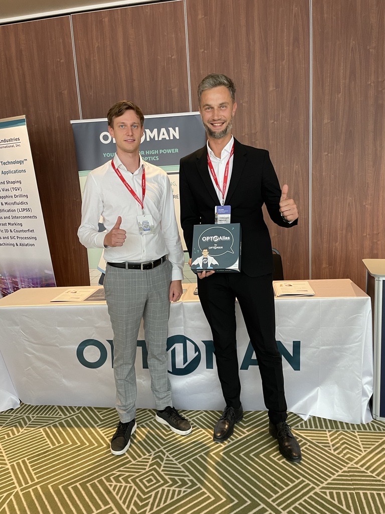
Big thank you to Dr. Mindaugas Gedvilas for his contribution to this article.
PARTNER WITH OPTOMAN
Building a laser micromachining system or scaling ablation processes to higher power? Contact OPTOMAN to discuss low-absorption optics for efficient, stable beam delivery.
Explore OPTOMAN products
REFERENCES
[1] G. Račiukaitis, M. Brikas, P. Gečys, B. Voisiat, M. Gedvilas, “Use of High Repetition Rate and High Power Lasers in Microfabrication: How to Keep the Efficiency High?,” J. Laser Micro/Nanoeng. 4(3), 186–191 (2009). https://doi.org/10.2961/jlmn.2009.03.0008
[2] A. Žemaitis, M. Gaidys, M. Brikas, P. Gečys, G. Račiukaitis, M. Gedvilas, “Advanced laser scanning for highly-efficient ablation and ultrafast surface structuring: experiment and model,” Sci. Rep. 8, 17376 (2018). https://doi.org/10.1038/s41598-018-35604-z
[3] A. Žemaitis, P. Gečys, M. Gedvilas, “Efficient Ablation, further GHz Burst Polishing, and Surface Texturing by Ultrafast Laser,” Adv. Eng. Mater. 26, 2302262 (2024). https://doi.org/10.1002/adem.202302262
[4] Lufthansa Technik, “AeroSHARK from Lufthansa Technik and BASF now certified for Boeing 777,” press release (December 16, 2022). https://newsroom.lufthansa-technik.com/aeroshark-from-lufthansa-technik-and-basf-now-certified-for-boeing-777/
[5] A. Papadopoulos, E. Skoulas, A. Mimidis, G. Perrakis, G. Kenanakis, G. D. Tsibidis, E. Stratakis, “Biomimetic Omnidirectional Antireflective Glass via Direct Ultrafast Laser Nanostructuring,” Adv. Mater. 31, 1901123 (2019). https://doi.org/10.1002/adma.201901123